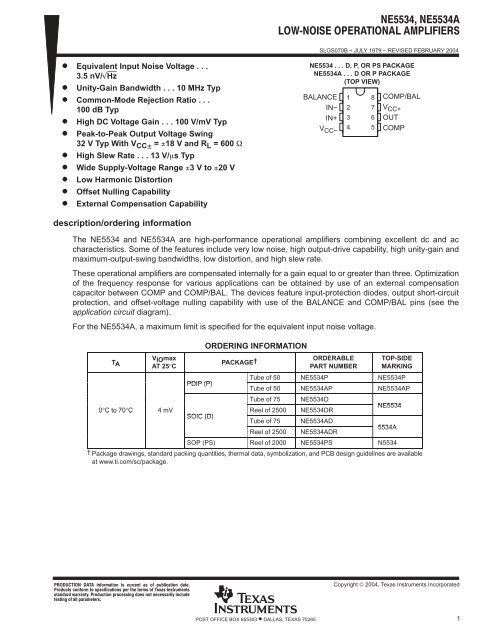
ne5534, ne5534a low noise operational amplifiers - AmpsLab.com
ne5534, ne5534a low noise operational amplifiers - AmpsLab.com
ne5534, ne5534a low noise operational amplifiers - AmpsLab.com

Create successful ePaper yourself
Turn your PDF publications into a flip-book with our unique Google optimized e-Paper software.
SLOS070B − JULY 1979 − REVISED FEBRUARY 2004<br />
Equivalent Input Noise Voltage . . .<br />
3.5 nV/Hz<br />
Unity-Gain Bandwidth . . . 10 MHz Typ<br />
Common-Mode Rejection Ratio . . .<br />
100 dB Typ<br />
High DC Voltage Gain . . . 100 V/mV Typ<br />
<br />
<br />
<br />
<br />
<br />
<br />
Peak-to-Peak Output Voltage Swing<br />
32 V Typ With V CC = 18 V and R L = 600 <br />
High Slew Rate . . . 13 V/s Typ<br />
Wide Supply-Voltage Range 3 V to 20 V<br />
Low Harmonic Distortion<br />
Offset Nulling Capability<br />
External Compensation Capability<br />
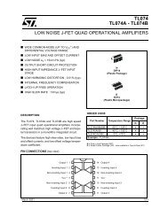
NE5534 ...D, P, OR PS PACKAGE<br />
NE5534A ...D OR P PACKAGE<br />
(TOP VIEW)<br />
BALANCE<br />
IN−<br />
IN+<br />
V CC−<br />
1<br />
2<br />
3<br />
4<br />
8<br />
7<br />
6<br />
5<br />
COMP/BAL<br />
V CC+<br />
OUT<br />
COMP<br />
description/ordering information<br />
The NE5534 and NE5534A are high-performance <strong>operational</strong> <strong>amplifiers</strong> <strong>com</strong>bining excellent dc and ac<br />
characteristics. Some of the features include very <strong>low</strong> <strong>noise</strong>, high output-drive capability, high unity-gain and<br />
maximum-output-swing bandwidths, <strong>low</strong> distortion, and high slew rate.<br />
These <strong>operational</strong> <strong>amplifiers</strong> are <strong>com</strong>pensated internally for a gain equal to or greater than three. Optimization<br />
of the frequency response for various applications can be obtained by use of an external <strong>com</strong>pensation<br />
capacitor between COMP and COMP/BAL. The devices feature input-protection diodes, output short-circuit<br />
protection, and offset-voltage nulling capability with use of the BALANCE and COMP/BAL pins (see the<br />
application circuit diagram).<br />
For the NE5534A, a maximum limit is specified for the equivalent input <strong>noise</strong> voltage.<br />
TA<br />
VIOmax<br />
AT 25°C<br />
0°C to 70°C 4 mV<br />
PDIP (P)<br />
SOIC (D)<br />
ORDERING INFORMATION<br />
PACKAGE†<br />
ORDERABLE<br />
PART NUMBER<br />
TOP-SIDE<br />
MARKING<br />
Tube of 50 NE5534P NE5534P<br />
Tube of 50 NE5534AP NE5534AP<br />
Tube of 75 NE5534D<br />
Reel of 2500 NE5534DR<br />
NE5534<br />
Tube of 75<br />
Reel of 2500<br />
NE5534AD<br />
NE5534ADR<br />
5534A<br />
SOP (PS) Reel of 2000 NE5534PS N5534<br />
† Package drawings, standard packing quantities, thermal data, symbolization, and PCB design guidelines are available<br />
at www.ti.<strong>com</strong>/sc/package.<br />
<br />
<br />
<br />
<br />
Copyright © 2004, Texas Instruments Incorporated<br />
POST OFFICE BOX 655303 • DALLAS, TEXAS 75265<br />
1
SLOS070B − JULY 1979 − REVISED FEBRUARY 2004<br />
schematic<br />
BALANCE<br />
1<br />
COMP/BAL<br />
COMP<br />
8 5 7<br />
VCC+<br />
100 pF<br />
12 kΩ<br />
12 kΩ<br />
IN+<br />
3<br />
40 pF<br />
15 Ω<br />
IN−<br />
2<br />
6<br />
OUT<br />
12 pF<br />
7 pF<br />
15 Ω<br />
4<br />
VCC−<br />
All <strong>com</strong>ponent values shown are nominal.<br />
symbol<br />
application circuit<br />
VCC+<br />
COMP<br />
COMP/BAL<br />
100 kΩ<br />
CC<br />
22 kΩ<br />
IN−<br />
IN+<br />
−<br />
+<br />
OUT<br />
2<br />
1<br />
8<br />
−<br />
5534<br />
5<br />
7<br />
6<br />
BALANCE<br />
3<br />
+<br />
4<br />
VCC−<br />
Frequency Compensation and Offset-Voltage Nulling Circuit<br />
2 POST OFFICE BOX 655303 • DALLAS, TEXAS 75265
SLOS070B − JULY 1979 − REVISED FEBRUARY 2004<br />
absolute maximum ratings over operating free-air temperature range (unless otherwise noted) †<br />
Supply voltage: V CC+ (see Note 1) . . . . . . . . . . . . . . . . . . . . . . . . . . . . . . . . . . . . . . . . . . . . . . . . . . . . . . . . . . . 22 V<br />
V CC− (see Note 1) . . . . . . . . . . . . . . . . . . . . . . . . . . . . . . . . . . . . . . . . . . . . . . . . . . . . . . . . . . −22 V<br />
Input voltage either input (see Notes 1 and 2) . . . . . . . . . . . . . . . . . . . . . . . . . . . . . . . . . . . . . . . . . . . . . . . . . V CC+<br />
Input current (see Note 3) . . . . . . . . . . . . . . . . . . . . . . . . . . . . . . . . . . . . . . . . . . . . . . . . . . . . . . . . . . . . . . . . ±10 mA<br />
Duration of output short circuit (see Note 4) . . . . . . . . . . . . . . . . . . . . . . . . . . . . . . . . . . . . . . . . . . . . . . . Unlimited<br />
Package thermal impedance, θ JA (see Notes 5 and 6): D package . . . . . . . . . . . . . . . . . . . . . . . . . . . . 97°C/W<br />
P package . . . . . . . . . . . . . . . . . . . . . . . . . . . . 85°C/W<br />
PS package . . . . . . . . . . . . . . . . . . . . . . . . . . . 95°C/W<br />
Operating virtual junction temperature, T J . . . . . . . . . . . . . . . . . . . . . . . . . . . . . . . . . . . . . . . . . . . . . . . . . . . 150°C<br />
Storage temperature range, T stg . . . . . . . . . . . . . . . . . . . . . . . . . . . . . . . . . . . . . . . . . . . . . . . . . . . −65°C to 150°C<br />
† Stresses beyond those listed under “absolute maximum ratings” may cause permanent damage to the device. These are stress ratings only, and<br />
functional operation of the device at these or any other conditions beyond those indicated under “re<strong>com</strong>mended operating conditions” is not<br />
implied. Exposure to absolute-maximum-rated conditions for extended periods may affect device reliability.<br />
NOTES: 1. All voltage values, except differential voltages, are with respect to the midpoint between VCC+ and VCC−.<br />
2. The magnitude of the input voltage must never exceed the magnitude of the supply voltage.<br />
3. Excessive current will f<strong>low</strong> if a differential input voltage in excess of approximately 0.6 V is applied between the inputs, unless some<br />
limiting resistance is used.<br />
4. The output may be shorted to ground or to either power supply. Temperature and/or supply voltages must be limited to ensure the<br />
maximum dissipation rating is not exceeded.<br />
5. Maximum power dissipation is a function of TJ(max), θ JA , and TA. The maximum al<strong>low</strong>able power dissipation at any al<strong>low</strong>able<br />
ambient temperature is PD = (TJ(max) − TA)/θ JA . Operating at the absolute maximum TJ of 150°C can affect reliability.<br />
6. The package thermal impedance is calculated in accordance with JESD 51-7.<br />
re<strong>com</strong>mended operating conditions<br />
MIN MAX UNIT<br />
VCC+ Supply voltage 5 15 V<br />
VCC− Supply voltage −5 −15 V<br />
POST OFFICE BOX 655303 • DALLAS, TEXAS 75265<br />
3
SLOS070B − JULY 1979 − REVISED FEBRUARY 2004<br />
electrical characteristics, V CC ± = ±15 V, T A = 25°C (unless otherwise noted)<br />
VIO<br />
Input offset voltage<br />
PARAMETER TEST CONDITIONS† MIN TYP MAX UNIT<br />
IIO Input offset current VO = 0<br />
IIB Input bias current VO = 0<br />
VO = 0,<br />
TA = 25°C 0.5 4<br />
RS = 50 Ω TA = Full range 5<br />
TA = 25°C 20 300<br />
TA = Full range 400<br />
TA = 25°C 500 1500<br />
TA = Full range 2000<br />
VICR Common-mode input voltage range ±12 ±13 V<br />
VO(PP) Maximum peak-to-peak output voltage swing RL ≥ 600 Ω<br />
AVD<br />
Large-signal differential voltage amplification<br />
Avd Small-signal differential voltage amplification f = 10 kHz<br />
BOM<br />
Maximum-output-swing bandwidth<br />
VCC± = ±15 V 24 26<br />
VCC± = ±18 V 30 32<br />
VO = ±10 V,<br />
TA = 25°C 25 100<br />
RL ≥ 600 Ω TA = Full range 15<br />
VO = ±10 V<br />
VCC± = ±18 V,<br />
RL ≥ 600 Ω,<br />
CC = 0 6<br />
CC = 22 pF 2.2<br />
CC = 0 200<br />
CC = 22 pF 95<br />
VO = ±14 V,<br />
CC = 22 pF<br />
B1 Unity-gain bandwidth CC = 22 pF, CL = 100 pF 10 MHz<br />
ri Input resistance 30 100 kΩ<br />
zo<br />
CMRR<br />
kSVR<br />
Output impedance<br />
Common-mode rejection ratio<br />
Supply-voltage rejection ratio (∆VCC/∆VIO)<br />
AVD = 30 dB,<br />
CC = 22 pF,<br />
VO = 0,<br />
RS = 50 Ω<br />
VCC+ = ±9 V to ±15 V,<br />
VO = 0<br />
RL ≥ 600 Ω,<br />
f = 10 kHz<br />
VIC = VICRmin,<br />
RS = 50 Ω,<br />
70<br />
mV<br />
nA<br />
nA<br />
V<br />
V/mV<br />
V/mV<br />
kHz<br />
0.3 Ω<br />
70 100 dB<br />
80 100 dB<br />
IOS Output short-circuit current 38 mA<br />
ICC Supply current VO = 0, No load TA = 25°C 4 8 mA<br />
† All characteristics are measured under open-loop conditions with zero <strong>com</strong>mon-mode input voltage, unless otherwise specified. Full range is<br />
TA = 0°C to 70°C.<br />
operating characteristics, V CC ± = ±15 V, T A = 25°C<br />
SR<br />
tr<br />
PARAMETER<br />
Slew rate<br />
Rise time<br />
Overshoot factor<br />
Rise time<br />
Overshoot factor<br />
TEST CONDITIONS<br />
NE5534<br />
TYP MIN<br />
NE5534A<br />
TYP MAX<br />
UNIT<br />
CC = 0 13 13<br />
CC = 22 pF 6 6<br />
V/µs<br />
VI I = 50 mV, AVD = 1,<br />
20 20 ns<br />
RL = 600 Ω,<br />
CC = 22 pF<br />
CL = 100 pF<br />
20 20 %<br />
VI I = 50 mV, AVD = 1,<br />
50 50 ns<br />
RL = 600 Ω,<br />
CC = 47 pF<br />
CL = 500 pF<br />
35 35 %<br />
f = 30 Hz 7 5.5 7<br />
Vn<br />
Equivalent input <strong>noise</strong> voltage<br />
f = 1 kHz 4 3.5 4.5 nV/√Hz<br />
f = 30 Hz 2.5 1.5<br />
In<br />
Equivalent input <strong>noise</strong> current<br />
pA/√Hz<br />
f = 1 kHz 0.6 0.4<br />
F Average <strong>noise</strong> figure RS = 5 kΩ, f = 10 Hz to 20 kHz 0.9 dB<br />
4 POST OFFICE BOX 655303 • DALLAS, TEXAS 75265
TYPICAL CHARACTERISTICS †<br />
SLOS070B − JULY 1979 − REVISED FEBRUARY 2004<br />
Normalized Input Bias Current and Input Offset Current<br />
1.6<br />
1.4<br />
1.2<br />
1<br />
0.8<br />
0.6<br />
NORMALIZED INPUT BIAS CURRENT<br />
AND INPUT OFFSET CURRENT<br />
vs<br />
FREE-AIR TEMPERATURE<br />
Bias<br />
Offset<br />
VCC± = ±15 V<br />
0.4<br />
−75 −50 −25 0 25 50 75 100 125<br />
TA − Free-Air Temperature − °C<br />
V O(PP) V OPP − Maximum Peak-to-Peak Output Voltage − V<br />
ÁÁÁ<br />
ÁÁÁ<br />
ÁÁÁ<br />
MAXIMUM PEAK-TO-PEAK OUTPUT VOLTAGE<br />
vs<br />
FREQUENCY<br />
30<br />
25<br />
20<br />
15<br />
10<br />
CC = 22 pF<br />
CC = 0<br />
5<br />
VCC± = ±15 V CC = 47 pF<br />
TA = 25°C<br />
0<br />
100 1 k 10 k 100 k 1 M<br />
f − Frequency − Hz<br />
Figure 1<br />
Figure 2<br />
VD − Differential Voltage Amplification − V/mV<br />
A<br />
106<br />
105<br />
104<br />
103<br />
102<br />
10<br />
LARGE-SIGNAL<br />
DIFFERENTIAL VOLTAGE AMPLIFICATION<br />
vs<br />
FREQUENCY<br />
VCC± = ±15 V<br />
TA = 25°C<br />
CC = 22 pF<br />
1<br />
10 100 1 k 10 k 100 k 1 M 10 M 100 M<br />
f − Frequency − Hz<br />
Figure 3<br />
CC = 0 pF<br />
Normalized Slew Rate and Unity-Gain Bandwidth<br />
1.2<br />
1.1<br />
1<br />
0.9<br />
0.8<br />
0.7<br />
0.6<br />
0.5<br />
TA = 25°C<br />
NORMALIZED SLEW RATE AND<br />
UNITY-GAIN BANDWIDTH<br />
vs<br />
SUPPLY VOLTAGE<br />
Unity-Gain<br />
Bandwidth<br />
0.4<br />
0 5 10 15 20<br />
| VCC± | − Supply Voltage − V<br />
Figure 4<br />
Slew Rate<br />
† Data at high and <strong>low</strong> temperatures are applicable only within the rated operating free-air temperature ranges of the various devices.<br />
POST OFFICE BOX 655303 • DALLAS, TEXAS 75265<br />
5
SLOS070B − JULY 1979 − REVISED FEBRUARY 2004<br />
TYPICAL CHARACTERISTICS †<br />
Normalized Slew Rate and Unity-Gain Bandwidth<br />
1.2<br />
1.1<br />
1<br />
0.9<br />
NORMALIZED SLEW RATE AND<br />
UNITY-GAIN BANDWIDTH<br />
vs<br />
FREE-AIR TEMPERATURE<br />
VCC± = ±15 V<br />
Unity-Gain<br />
Bandwidth<br />
Slew Rate<br />
0.8<br />
−75 −50 −25 0 25 50 75 100 125<br />
TA − Free-Air Temperature − °C<br />
THD − Total Harmonic Distortion − %<br />
0.01<br />
0.007<br />
0.004<br />
0.002<br />
0.001<br />
100 400 1 k<br />
TOTAL HARMONIC DISTORTION<br />
vs<br />
FREQUENCY<br />
VCC± = ±15 V<br />
AVD = 1<br />
VI(rms) = 2 V<br />
TA = 25°C<br />
f − Frequency − Hz<br />
4 k 10 k 40 k 100 k<br />
Figure 5<br />
Figure 6<br />
Vn − Equivalent Input Noise Voltage − nV/ Hz<br />
10<br />
7<br />
4<br />
2<br />
EQUIVALENT INPUT NOISE VOLTAGE<br />
vs<br />
FREQUENCY<br />
1<br />
10 100<br />
1 k 10 k 100 k<br />
f − Frequency − Hz<br />
VCC± = ±15 V<br />
TA = 25°C<br />
SE5534, NE5534<br />
SE5534A, NE5534A<br />
I n − Equivalent Input Noise Current − pA/ Hz<br />
10<br />
7<br />
4<br />
2<br />
1<br />
0.7<br />
0.4<br />
0.2<br />
EQUIVALENT INPUT NOISE CURRENT<br />
vs<br />
FREQUENCY<br />
VCC± = ±15 V<br />
TA = 25°C<br />
SE5534, NE5534<br />
SE5534A, NE5534A<br />
0.1<br />
10 100 1 k 10 k 100 k<br />
f − Frequency − Hz<br />
Figure 7<br />
Figure 8<br />
† Data at high and <strong>low</strong> temperatures are applicable only within the rated operating free-air temperature ranges of the various devices.<br />
6 POST OFFICE BOX 655303 • DALLAS, TEXAS 75265
TYPICAL CHARACTERISTICS<br />
SLOS070B − JULY 1979 − REVISED FEBRUARY 2004<br />
µV<br />
Total Equivalent Input Noise Voltage −<br />
100<br />
70<br />
40<br />
20<br />
10<br />
7<br />
4<br />
2<br />
1<br />
0.7<br />
0.4<br />
0.2<br />
TOTAL EQUIVALENT INPUT NOISE VOLTAGE<br />
vs<br />
SOURCE RESISTANCE<br />
VCC± = ±15 V<br />
TA = 25°C<br />
f = 10 Hz to 20 kHz<br />
f = 200 Hz to 4 kHz<br />
0.1<br />
100 1 k 10 k 100 k 1 M<br />
RS − Source Resistance − Ω<br />
Figure 9<br />
POST OFFICE BOX 655303 • DALLAS, TEXAS 75265<br />
7
MECHANICAL DATA<br />
MCER001A – JANUARY 1995 – REVISED JANUARY 1997<br />
JG (R-GDIP-T8)<br />
CERAMIC DUAL-IN-LINE<br />
0.400 (10,16)<br />
0.355 (9,00)<br />
8<br />
5<br />
0.280 (7,11)<br />
0.245 (6,22)<br />
1<br />
4<br />
0.065 (1,65)<br />
0.045 (1,14)<br />
0.063 (1,60)<br />
0.015 (0,38)<br />
0.020 (0,51) MIN<br />
0.310 (7,87)<br />
0.290 (7,37)<br />
0.200 (5,08) MAX<br />
Seating Plane<br />
0.130 (3,30) MIN<br />
0.100 (2,54)<br />
0.023 (0,58)<br />
0.015 (0,38)<br />
0.014 (0,36)<br />
0.008 (0,20)<br />
0°–15°<br />
4040107/C 08/96<br />
NOTES: A. All linear dimensions are in inches (millimeters).<br />
B. This drawing is subject to change without notice.<br />
C. This package can be hermetically sealed with a ceramic lid using glass frit.<br />
D. Index point is provided on cap for terminal identification.<br />
E. Falls within MIL STD 1835 GDIP1-T8<br />
POST OFFICE BOX 655303 • DALLAS, TEXAS 75265
MECHANICAL DATA<br />
MPDI001A – JANUARY 1995 – REVISED JUNE 1999<br />
P (R-PDIP-T8)<br />
PLASTIC DUAL-IN-LINE<br />
8<br />
0.400 (10,60)<br />
0.355 (9,02)<br />
5<br />
0.260 (6,60)<br />
0.240 (6,10)<br />
1<br />
4<br />
0.070 (1,78) MAX<br />
0.020 (0,51) MIN<br />
0.325 (8,26)<br />
0.300 (7,62)<br />
0.015 (0,38)<br />
0.200 (5,08) MAX<br />
Gage Plane<br />
Seating Plane<br />
0.125 (3,18) MIN<br />
0.010 (0,25) NOM<br />
0.021 (0,53)<br />
0.015 (0,38)<br />
0.100 (2,54)<br />
0.010 (0,25)<br />
M<br />
0.430 (10,92)<br />
MAX<br />
4040082/D 05/98<br />
NOTES: A. All linear dimensions are in inches (millimeters).<br />
B. This drawing is subject to change without notice.<br />
C. Falls within JEDEC MS-001<br />
For the latest package information, go to http://www.ti.<strong>com</strong>/sc/docs/package/pkg_info.htm<br />
POST OFFICE BOX 655303 • DALLAS, TEXAS 75265
IMPORTANT NOTICE<br />
Texas Instruments Incorporated and its subsidiaries (TI) reserve the right to make corrections, modifications,<br />
enhancements, improvements, and other changes to its products and services at any time and to discontinue<br />
any product or service without notice. Customers should obtain the latest relevant information before placing<br />
orders and should verify that such information is current and <strong>com</strong>plete. All products are sold subject to TI’s terms<br />
and conditions of sale supplied at the time of order acknowledgment.<br />
TI warrants performance of its hardware products to the specifications applicable at the time of sale in<br />
accordance with TI’s standard warranty. Testing and other quality control techniques are used to the extent TI<br />
deems necessary to support this warranty. Except where mandated by government requirements, testing of all<br />
parameters of each product is not necessarily performed.<br />
TI assumes no liability for applications assistance or customer product design. Customers are responsible for<br />
their products and applications using TI <strong>com</strong>ponents. To minimize the risks associated with customer products<br />
and applications, customers should provide adequate design and operating safeguards.<br />
TI does not warrant or represent that any license, either express or implied, is granted under any TI patent right,<br />
copyright, mask work right, or other TI intellectual property right relating to any <strong>com</strong>bination, machine, or process<br />
in which TI products or services are used. Information published by TI regarding third-party products or services<br />
does not constitute a license from TI to use such products or services or a warranty or endorsement thereof.<br />
Use of such information may require a license from a third party under the patents or other intellectual property<br />
of the third party, or a license from TI under the patents or other intellectual property of TI.<br />
Reproduction of information in TI data books or data sheets is permissible only if reproduction is without<br />
alteration and is ac<strong>com</strong>panied by all associated warranties, conditions, limitations, and notices. Reproduction<br />
of this information with alteration is an unfair and deceptive business practice. TI is not responsible or liable for<br />
such altered documentation.<br />
Resale of TI products or services with statements different from or beyond the parameters stated by TI for that<br />
product or service voids all express and any implied warranties for the associated TI product or service and<br />
is an unfair and deceptive business practice. TI is not responsible or liable for any such statements.<br />
Fol<strong>low</strong>ing are URLs where you can obtain information on other Texas Instruments products and application<br />
solutions:<br />
Products<br />
Applications<br />
Amplifiers amplifier.ti.<strong>com</strong> Audio www.ti.<strong>com</strong>/audio<br />
Data Converters dataconverter.ti.<strong>com</strong> Automotive www.ti.<strong>com</strong>/automotive<br />
DSP dsp.ti.<strong>com</strong> Broadband www.ti.<strong>com</strong>/broadband<br />
Interface interface.ti.<strong>com</strong> Digital Control www.ti.<strong>com</strong>/digitalcontrol<br />
Logic logic.ti.<strong>com</strong> Military www.ti.<strong>com</strong>/military<br />
Power Mgmt power.ti.<strong>com</strong> Optical Networking www.ti.<strong>com</strong>/opticalnetwork<br />
Microcontrollers microcontroller.ti.<strong>com</strong> Security www.ti.<strong>com</strong>/security<br />
Telephony<br />
www.ti.<strong>com</strong>/telephony<br />
Video & Imaging www.ti.<strong>com</strong>/video<br />
Wireless<br />
www.ti.<strong>com</strong>/wireless<br />
Mailing Address:<br />
Texas Instruments<br />
Post Office Box 655303 Dallas, Texas 75265<br />
Copyright © 2004, Texas Instruments Incorporated