


Introduction
The IC 555 timer was invented in 1971 by “Hans Camenzind” at Signetic Corporation and it was named SE or NE 555 timer. These types of ICs are very cheap & reliable in cost & size, when compared to other IC example OP-Amp in the same areas.

These ICs are used as astable and mono-stable multi-vibrators in digital logic probes, DC-DC converters, tachometers, analog frequency meters, voltage regulators, temperature-controlled & measurement devices. The SE 555 Timer IC works between the temperature range of – 55°C to 125°C in SE and the IC NE 555 is used for where the temperature ranges from 0° to 70°C. It has a wide range of usages in the electronic field as a timer, delay, pulse generation, oscillator, etc.
You can check the datasheet of NE555 IC if you want to learn more about it.
Design, Construction, Architecture & Working
The IC 555 timer is a chip used in various areas and applications like pulse generation, an oscillator, and a timer. The 555 Timer is designed using 25 transistors, 2 diodes and 15 resistors.

The functional parts of the 555 timer IC include a flip-flop, voltage divider & a comparator altogether. The main function of this IC is to generate an accurate timing pulse for operating various devices and electronic components.

The voltage divider consists of three 5k resistors which create two reference voltages. The reference voltages are 1/3 and 2/3 of the supplied voltage that ranges from 5 to 15V.
Then, there are two comparators that compare two analog voltages. If the input voltage at the positive terminal is higher than the input voltage at the negative terminal the comparator will output 1. Similarly, if the voltage at the negative input terminal is higher than the voltage at the positive terminal, the comparator will output 0.
The first comparator -ve input terminal is connected to the 2/3 reference voltage at the voltage divider and the external control pin, while the +ve input terminal to the external Threshold pin. The second comparator -ve input terminal is connected to the Trigger pin, while the +ve input terminal to the 1/3 reference voltage at the voltage divider.
So using the three pins Trigger, Threshold & Control, we can control the output of the two comparators. The output is then fed to the R and S inputs of the flip-flop. The flip-flop will output 1 when R is 0 and S is 1 or vice versa. The flip-flop can be reset via the external pin called Reset which can override the two inputs, thus resetting the entire timer at any time.
The Q-bar output of the flip-flip goes to the output stage or the output drivers which can either source or sink a current of 200mA to the load. The output of the flip-flip is also connected to a transistor that connects the Discharge pin to the ground.
555 Timer IC Pinout
The 555 Timer IC has 8 Pins which are explained below in detail.

Pin 1: GND Pin
Ground pin directly connected to the negative terminal of the power source. It is suggested that it should not be connected using any resistor because all the IC will heat up due to stray voltage (it is the occurrence of electrical potential between any two objects that ideally should not have any voltage difference between them at all) in it.
Pin 2: Trigger Pin
A trigger pin is used to activate the IC’s timing cycle for operating. It is a low signal pin and the timer is triggered when the voltage is below one-third of the supply voltage (1/3 V). It is connected to the Inverting input of the comparator inside the IC and accepts negative signals for the operation.
Pin 3: Output Pin
It is the output pin. As the IC triggered the output pin goes high depending on the duration of the timing cycle provided to it. In the case of logic zero o/p; it is a sinking current with voltage greater than zero (0 V). Whereas, in the case of logic high output, it is sourcing current with the output voltage lesser than Vcc.
Pin 4: Reset Pin
The reset pin is used to reset. It should be connected to the positive terminal to work the IC properly. If this pin is grounded, the IC won’t work at all. The required reset voltage is 0.7 volts at a current rating of 0.1mA to work.
Pin 5: Control Voltage
It is used for reliable operation. When not in use, it should be connected to the ground through a capacitor; otherwise, the IC will show erratic responses (deviating from the desired value).
Pin 6: Threshold Pin
It detects when the voltage on the timing capacitor rises above 0.66Vcc. The timing cycle is only completed when the voltage on this particular pin is equal to or greater than 2/3 of Vcc.
Pin 7: Discharge pin
It is used to provide a discharge path from the timing capacitor to the ground when the output is low. The discharging current should be less than 50 mA in order to prevent it from damaged.
Pin 8: Supply Terminal
It is a positive (+ve) terminal that is connected to the positive terminal of the power supply in order to power up. It is used to take power supply voltage from the power source for operating.
Operating Modes of 555 Timer IC
1. Astable Mode
In this mode, the circuit of the IC 555 timer produces continuous pulses with exact frequency based on the value of the resistors and capacitors. Here, the charging and discharging of the capacitors depends on voltage.

The square wave is produced at the output pin and this wave is used to turn ON and OFF a load at specific intervals like blinking by producing delay. In the astable mode, both the duty cycle & frequency are controlled by two external resistors and one capacitor for the desired operation.

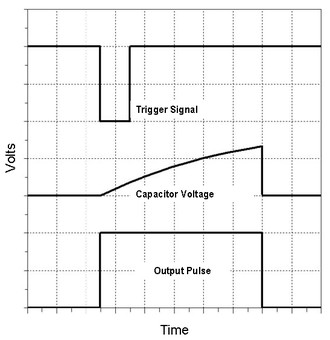
2. Mono-stable Mode
In the mono-stable mode, the circuit generates only a single pulse when the timer gets an indication from the input of the trigger button. Pulse duration usually depends on the resistor and capacitor values.

If it is applied to the input of the circuit through the use of a push-button, then the capacitor gets charged and the timer circuit extends a high pulse, then it remains high until the capacitor totally gets discharge. If it is necessary to enhance the time delay, then a higher rate of capacitor and resistor are required as necessary.
3. Bi-stable Mode
Bi-stable mode is also known as Schmitt Trigger Mode. It is used when a load has to be turned on and off continuously and it did with the help of a push-button.

Here the circuit produces two stable state signals which are low and states. The output signals of low and high state signals are controlled by reset & activate the input pins, not by the charging & discharging of capacitors. If a low logic signal is given to the active pin, then the output of the IC circuit goes to a high level. If the low logic signal is given to the RST pin, then the output of the circuit goes to a low level.

Features of the 555 Timer IC
• It can be operated in +5V, can withstand up to +18V.
• The source and sink current of the output pin is near about 200mA.
• Trigger Voltage is 1.6 when operating at +5V.
• Operating Temperature is near about 70 degrees Celsius.
• It is available in 8-pin PDIP, SOIC, and VSSOP packages.
• The duty cycle of the 555 timers can be variable as per user need.
Applications
The 555 timer is one of the most widely used integrated chips in digital electronics. Some common uses and application of 555 timers IC are as follows:
• It is used for Pulse, Waveform, and square wave generation.
• It is also used in time delay generation, precision timing, and sequential timing.
• It can be used as a mono-stable multi-vibrator and a-stable multi-vibrator.
• It is mostly used in PWM (Pulse Width Modulation) & PPM (Pulse Position Modulation).
• Used in Tachometers & temperature measurement.
• Commonly used in DC Voltage Regulators.
• Used for conversion like Voltage to Frequency Converter.
• It is also used in Frequency Divider.
• It is used in the Pulse detector.
• It can be used to design a Timer Switch.
We have made multiple projects using 555 Timer IC. You can follow up the 555 Timer Based Projects section to understand more about the 555 Timer IC. All the projects presented will help you to boost your knowledge.
 – PCB Design & Analysis")


